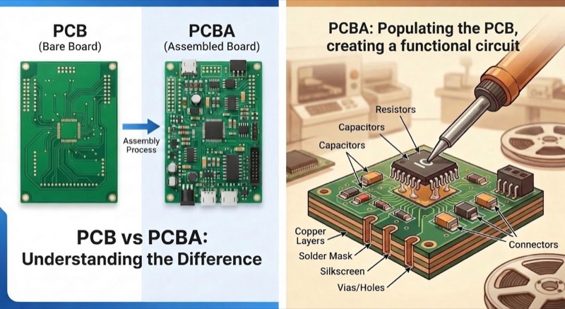
Short answer: a PCB is the bare board — an insulating substrate with etched copper and nothing mounted on it. A PCBA is that same board after components have been soldered onto it, a functional circuit ready for test and integration. PCB and PCBA are two consecutive stages of electronics manufacturing: built on different equipment, quoted from different files, governed by different specifications, and inspected against different criteria.
The two words get used interchangeably in day-to-day conversation, and most of the time nobody is harmed by it. The exception is the moment you send an inquiry to a manufacturer, because at that point the word you chose decides what gets quoted. This article defines each stage, shows exactly where fabrication ends and assembly begins, and clears up the vocabulary — bare board, PWB, CCA, SMT — that produces most of the confusion.
PCB vs PCBA at a glance
| Dimension | PCB (bare board) | PCBA (assembled board) |
|---|---|---|
| What it is | Substrate, copper, mask and finish — an empty platform | That platform with every component soldered in place |
| How it is made | Fabrication: imaging, etching, lamination, drilling, plating | Assembly: paste printing, placement, reflow, wave or selective soldering |
| Files that define it | Gerber or ODB++, drill data, board specification | All of that, plus BOM and pick-and-place (centroid) file |
| What verification proves | The copper matches the netlist | The circuit behaves as designed |
| What you can do with it | Send it to assembly | Power it up and integrate it into a product |
| Also called | Bare board, blank board, unpopulated board, PWB | Populated board, loaded board, assembled PCB, CCA, PBA |
What is a PCB? The bare board
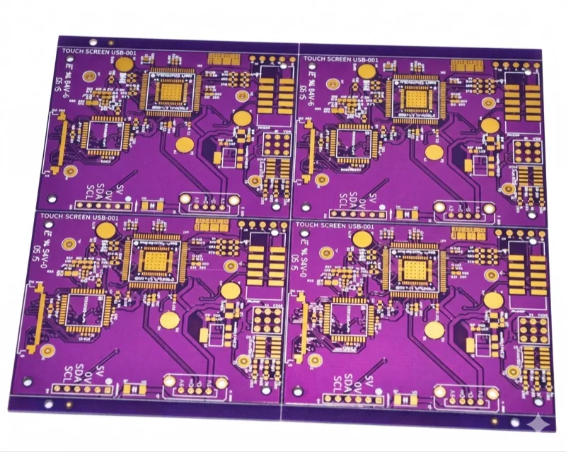
A Printed Circuit Board (PCB) is the structural foundation of an electronic device: insulating material — most commonly fiberglass-reinforced epoxy laminate (FR-4), but also Polyimide for flex circuits, aluminum for thermal management, or high-frequency laminates such as Rogers — carrying etched copper traces that will connect the components.
A PCB by itself contains no components. It provides the conductive pathways and the mounting structure for a circuit that does not exist yet. Typical elements:
- Copper layers — one layer up to 42 in advanced multilayer designs, separated by core and prepreg.
- Solder mask — the coating (green by convention, any color on request) that prevents shorts and defines where solder may flow.
- Silkscreen — printed reference designators and polarity marks.
- Vias and holes — plated connections between layers, plus holes for through-hole parts and mounting.
- Surface finish — HASL, lead-free HASL, ENIG, immersion silver or immersion tin, protecting the exposed pads until they are soldered.
Producing the bare board is called PCB fabrication: DFM review, imaging and etching, lamination, drilling, plating and surface finish, solder mask and silkscreen, then electrical test and inspection. To quote it, a fabricator needs only your Gerber (or ODB++) data and a note on stack-up, material and finish.
One detail explains much of what follows. The electrical test at the end of fabrication verifies that the copper matches the netlist — not that the circuit works, because at this point there is no circuit. There is a platform waiting for one.
What is a PCBA? The assembled board
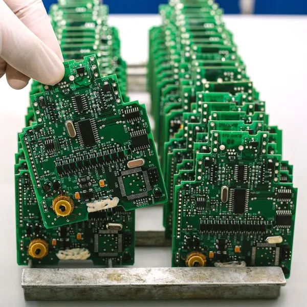
PCBA (Printed Circuit Board Assembly) is both the process and the resulting product: components assembled onto a bare PCB. Resistors, capacitors, integrated circuits and connectors are soldered on to create a working circuit.
Modern PCB assembly combines two soldering technologies, usually on the same board:
- SMT (Surface Mount Technology) — solder paste is stencil-printed onto the pads, components are placed into it by high-speed pick-and-place machines, and the board passes through a reflow oven. This handles most modern parts, from 0201/01005 passives to fine-pitch BGAs, across DIP, SOP, QFP, PGA, BGA and CSP package families.
- THT (Through-Hole Technology) — component leads pass through plated holes and are wave-soldered or selectively soldered. Still standard for connectors and parts that take mechanical abuse.
Assembly also pulls in work that has nothing to do with soldering: component procurement, solder paste inspection (SPI), automated optical inspection (AOI), X-ray on hidden joints, and electrical test. That is why quoting a PCBA needs more from you than quoting a bare board — a Bill of Materials and a pick-and-place file on top of the Gerbers.
The other thing that changes is that a PCBA can be exercised. A bare board is checked for continuity and isolation; an assembly can be powered up, which is why in-circuit and functional testing only enter the conversation at this stage.
Where PCB fabrication ends and PCBA assembly begins
The clearest proof that these are two different processes is that a manufacturer publishes two separate capability lists for them, and a number from one list means nothing on the other. The same physical board is governed by the fabrication list while it is being built, and by the assembly list once it reaches an SMT line. Below are BELI's two lists side by side.
| Parameter | Fabrication spec (governs the bare PCB) | Assembly spec (governs the PCBA) |
|---|---|---|
| Size | Panels up to 18 × 24 inches — the production panel that boards are stepped into | Boards from 45 × 45 mm to 680 × 500 mm, as a single board or an array |
| Board thickness | 0.2 mm – 8.0 mm | 0.4 mm – 5 mm |
| Layer count | Up to 42 layers — decided entirely at fabrication | Inherited from the board |
| Fine-feature limits | 3.0/3.0 mil inner and 4.0/4.0 mil outer line width and spacing; 4 mil minimum hole; 11:1 maximum aspect ratio | Components down to 0201/01005; 0.35 mm minimum lead pitch; 0.4 mm minimum BGA ball pitch; components up to 25 mm tall |
| Precision that matters | Impedance control ±10% | Placement precision ±0.03 mm |
| Materials | FR-4, High-Tg FR-4, halogen-free, Rogers, Arlon, Taconic, Nelco; copper weight 0.5 – 6.0 oz | Inherited from the board — the surface finish chosen at fabrication is what the solder has to wet |
| Capacity is counted in | Panels | Placements — roughly 52 million per month |
Read the table the right way round and two familiar misunderstandings disappear. The 18 × 24 inch figure describes the fabrication panel, not the largest board that can be built; a 500 × 400 mm board is stepped into that panel during fabrication and sits comfortably inside the 680 × 500 mm assembly envelope afterwards. And thickness is stated twice for the same board — 0.2 to 8.0 mm at fabrication, 0.4 to 5 mm on the SMT line — because the number that matters changes with the machine holding it. Check a borderline design against the list that governs that stage; the manufacturing capability page keeps the two sets separate for exactly this reason.
PCB and PCBA quotes need different files
A bare-board quote is a geometry-and-materials question. An assembly quote is a parts-and-orientation question layered on top of it. Sending the wrong package for your scope is the most common reason a first quote comes back wrong.
| What you send | Bare PCB quote | PCBA quote |
|---|---|---|
| Gerber (RS-274X) or ODB++, with drill data and board outline | Required — this is the quote | Required; it also cuts the stencil and defines depanelization |
| Stack-up, material, copper weight, finish, mask color | Required; these set the board price | Same, and the finish affects solderability |
| BOM with manufacturer part numbers | Belongs to the assembly package | Required; drives most of the price and the lead time |
| Pick-and-place / centroid file | Belongs to the assembly package | Required; X, Y, rotation and layer for every placed part |
| Assembly drawing or build notes | Belongs to the assembly package | Resolves polarity, orientation and hand-fitted parts |
Because the two packages are read by different people against different rules, the manufacturability check runs twice: BELI includes DFM analysis with every fabrication order and runs a separate assembly DFM review before the line is set up. Our guides to exporting a complete Gerber package and to the files required for a PCBA quotation cover what each file has to contain.
How PCB and PCBA costs are built up
A bare PCB is priced on physics and area: layer count, panel utilization, base material, copper weight, minimum feature size, surface finish and quantity. A four-layer FR-4 board with ENIG costs what it costs before anyone reads your schematic.
A PCBA is priced in three stacked layers — the bare board, the components, and the labor and machine time to assemble them and prove they work. For most assembled products the bare board is a minor share; components usually dominate, followed by assembly, setup and test. That is why a BOM with real manufacturer part numbers moves a PCBA quote far more than a change of solder mask color does.
The trap when comparing suppliers is scope. A bare-board quote and a finished-assembly quote are not comparable numbers, and neither are a turnkey quote (the manufacturer buys the parts) and a consignment quote (you buy them, and only assembly is priced). Our breakdown of what PCBA costs in China and the comparison of turnkey versus consignment assembly work through the arithmetic.
PCB vs PCBA lead times: two different clocks
The two stages run on different clocks, and mixing them up produces impossible schedules. Bare-board fabrication is process-bound — the chemistry and the presses take the time they take. Assembly is procurement-bound, because parts, not placement, set the date.
At BELI, bare-board fabrication runs as fast as 24 hours for 1–2 layer boards and typically 3–7 working days for multilayer designs. Quick-turn prototype assembly takes 48 hours once boards and components are on site. A turnkey order in which the manufacturer also buys the components typically takes 2 to 3 weeks in total, because component sourcing — standard parts in 3–7 days through authorized distributors and original manufacturers — is the long pole.
So the honest answer to "how long does a PCBA take" is: bare-board time, plus parts time, plus assembly time, plus your test plan. A 48-hour figure describes the machine, not the project — a distinction that EVT, DVT and PVT schedules live or die on, and one that also drives the gap between prototype and mass production cost.
How a PCB and a PCBA are inspected
Inspection is where the two stages diverge most sharply, simply because there is more to look at once components are present.
| What is checked | On the bare PCB | On the PCBA |
|---|---|---|
| Conductor integrity | Electrical test against the netlist | Re-checked through node access during in-circuit test |
| Surface and feature quality | Visual and AOI inspection before shipment | AOI after reflow: presence, polarity, alignment |
| Solder paste and joints | Belongs to the assembly stage | SPI before placement; X-ray for BGA and QFN joints |
| Circuit function | Verified after components are on the board | ICT, flying probe, or functional test against your spec |
| Early-life reliability | Belongs to the assembly stage | Burn-in and environmental stress screening |
| Evidence you receive | Boards that passed electrical test and AOI | Test reports covering the assembled boards |
Put numbers against that and the split becomes concrete. At BELI, every bare board is electrically tested and AOI-inspected before shipment. On the assembly side, AOI and X-ray run on every order with first-pass yield held at 99.5% or better, ICT reaches 95% node coverage or higher, flying probe covers prototypes and small batches where a dedicated fixture is not yet economical, and custom test fixtures are built in 2–3 working days. Optional burn-in runs up to 24 hours, and environmental stress screening covers −40 to +85 °C at 20–98% RH. Test reports are delivered with every shipment.
When a board fails, which stage owns it
Split the two stages across two vendors and you split the diagnosis with them. A dead board can be a fabrication issue — a broken via barrel, a registration error, a contaminated finish that would not wet — or an assembly issue: a cold joint, a tombstoned part, a wrong-value reel. Both parties can honestly report that their inspection passed, because each measured a different data set: the fabricator against your Gerbers, the assembler against your BOM and centroid file.
Keeping both stages with one supplier collapses that triage into one conversation. BELI runs fabrication, sourcing, assembly and testing under one roof, so DFM review covers the board data and the assembly data, and component traceability is maintained through the supply chain with 100% visual inspection plus X-ray sampling on incoming parts.
What arrives in the box: bare boards vs assemblies
A bare-board order arrives as individual routed boards, or as panels with breakaway tabs or V-scoring. If those boards are going onto an SMT line, panel format is not cosmetic: tooling rails, fiducials and edge clearance are what let a machine hold and register the board. When fabrication and assembly sit with two vendors, somebody has to own the panel drawing between them.
A PCBA order arrives as inspected, tested assemblies. Value-added work may already be done: conformal coating or potting for harsh environments, or a complete box build with the assembly already mated to its harness and enclosure.
PCB, PWB, PCBA, CCA: the vocabulary that trips buyers up
Much of the PCB versus PCBA confusion is terminology rather than engineering. These are the terms that show up in real inquiries, and where each one sits.
| Term | What it means | Where it sits relative to PCB / PCBA |
|---|---|---|
| Bare board, blank board, unpopulated board | The board before any component is attached | All three mean PCB |
| PWB (printed wiring board) | The older name for the bare board, still seen in legacy drawings | Means PCB |
| CCA (circuit card assembly) | Common in aerospace, defense and older industrial documentation | Means PCBA — prepare a BOM and centroid file exactly as you would for one |
| PBA, populated board, loaded board | Shop-floor and drawing-office variants for a board with parts on it | All mean PCBA |
| SMD (surface mount device) | The component itself — a resistor, capacitor or IC in a surface-mount package | A part that gets placed onto a PCB during assembly |
| SMT (surface mount technology) | The printing, placement and reflow process | One process inside PCBA, which also covers through-hole work, inspection and test |
| Daughterboard, mezzanine, module | A smaller board that plugs into a larger one through a connector | Two PCBAs joined together — not one board printed on another |
| "PCB manufacturer" | Used loosely for a board fabricator, an assembly house, or a company that does both | Ambiguous — this is where most sourcing mix-ups begin |
The practical fix is one sentence at the top of your inquiry. State whether you are buying bare boards (PCB), assembly of components you supply (consignment PCBA), or finished boards including the parts (turnkey PCBA). Naming the scope up front removes a round trip before anyone has opened a file.
Where PCBs and PCBAs are used
Both sit at the core of consumer electronics, industrial automation, medical devices, robotics, IoT and telecommunications. Which stage you buy depends on where you sit in the chain: a contract assembler buys bare boards, a product company usually buys assemblies. Regulated sectors add documentation on top of the hardware. The boards we ship are built at partner manufacturing facilities certified to ISO 9001:2015, ISO 14001 and ISO 13485:2016; certificate copies (registrar, certified site, validity dates) are provided on request with any RFQ. Materials and processes are RoHS- and REACH-compliant, and our medical device PCB assembly page sets out which manufacturing records travel with the boards and which parts of the file stay with you.
Do you need a PCB or a PCBA?
Work backwards from what you want to hold:
- Bare PCBs if you assemble in house or already have an assembler. Send Gerber or ODB++ plus your board specification.
- PCBA if you want boards that work. Then pick the commercial model: turnkey, where the manufacturer buys the BOM, or consignment, where you supply the parts. Both are supported, with no fixed ratio between them.
- Box build if you want a finished unit — assembly plus harness, enclosure and final testing.
PCB and PCBA are two stages of one journey: the PCB provides the physical structure, and assembly turns it into a functional electronic product. BELI Technologies provides both — PCB fabrication up to 42 layers and turnkey PCBA with AOI, X-ray and ICT — under one roof, from a single prototype with no MOQ through to volume production. Send us your files and our engineers will scope it with you; quotes are returned within 24 hours on business days.
Common questions about PCB and PCBA
Is a PCBA the same as a finished product?
Not usually. A PCBA is a tested board. Turning it into something you can ship — enclosure, harness, panel work, labeling, final functional test and packing — is box build, a separate stage with its own drawings and specifications.
Is SMT the same as PCBA?
SMT is one of the soldering technologies used during assembly. PCBA is the whole job: SMT plus through-hole work, inspection and test. A board can be assembled with SMT alone, with through-hole alone, or with both, and it is a PCBA in every case.
Can one supplier handle both PCB and PCBA?
Yes, and that is what a one-stop EMS provider means: fabrication, component sourcing, assembly and testing run under one roof, so a single team owns the finished, working board. Our guide to what one-stop EMS actually means covers how to verify the claim rather than take it at face value.
Related reading: What Files Are Required for PCBA Quotation · How Much Does PCBA Cost in China · Turnkey vs Consignment PCB Assembly