
Production Capability
PCB & SMT Manufacturing Capability
Up to 42-layer PCB · ±0.03mm precision · 52 million placements per month.
Manufacturing Capacity
PCB Production Capabilities
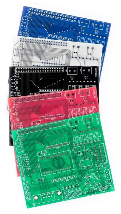
BELI fabricates 1 to 42 layer boards in FR-4, High-Tg, polyimide, aluminium, ceramic and Rogers laminates, with impedance control to ±10%. Full details on the PCB fabrication service page.
- Layers
- Up to 42
- Min Line Width/Spacing (Inner)
- 3.0/3.0 mil
- Min Line Width/Spacing (Outer)
- 4.0/4.0 mil
- Copper Weight
- 0.5 – 6.0 OZ
- Max Aspect Ratio
- 11:1
- Board Thickness
- 0.2mm – 8.0mm
- Max Panel Size
- 18″ × 24″
- Min Hole Diameter
- 4 mil
- Material
- FR-4, High Tg FR-4, Halogen free, Rogers, Arlon, Taconic, Nelco
- Surface Treatment
- HASL, ENIG, Immersion Silver, Immersion Tin, Lead free HASL
- Impedance Control
- +/-10%
SMT Production
SMT Production Capabilities
Around 52 million placements per month at ±0.03 mm accuracy, down to 0201/01005 parts and 0.4 mm BGA pitch, on boards up to 680 × 500 mm. See the PCB assembly service, or how these capabilities map to build stages in EVT, DVT and PVT.

| Max PCB Size | 680 × 500 mm |
|---|---|
| Min PCB Size | 45 × 45 mm |
| Board Thickness | 0.4 – 5 mm |
| Min Components Size | 0201 / 01005 |
| Component Max Height | 25 mm |
| Min Lead Pitch | 0.35 mm |
| Min BGA Ball Pitch | 0.4 mm |
| Placement Precision | +/- 0.03 mm |
Our Equipment
Advanced Equipment
AOI Machine
Automated optical inspection for 100% surface defect detection on all assemblies
X-Ray Machine
Real-time X-ray inspection for BGA, QFN, and hidden solder joint verification
SMT Pick & Place
High-speed component placement at 0.15 seconds per chip with ±0.03mm precision
Reflow Oven
Nitrogen-atmosphere reflow soldering with 10-zone temperature profile control
Wave Solder
Lead-free wave soldering for through-hole and mixed technology assemblies
ICT Testing
In-circuit testing with custom fixtures for 100% electrical verification
FAQ
Frequently Asked Questions
What is BELI's maximum PCB layer count and technology range?
What is the minimum line width and spacing?
What is the smallest component and BGA pitch your SMT lines can place?
What PCB materials do you support?
What is your monthly SMT capacity and board size range?
What surface finishes are available?
What inspection and testing capabilities do you have?
What copper weights and board thicknesses can you fabricate?
Get In Touch
Get your PCBA quote within 24 hours
Send your design files — Gerber, BOM and pick-and-place, or drawings and wire lists for harness work — attach them directly in the form (up to 5 files, 25 MB each) and an engineer will come back with a quotation within 24 hours, 7 days a week. No MOQ for prototypes · 48-hour quick-turn prototype assembly · ≥99.5% first-pass yield.