
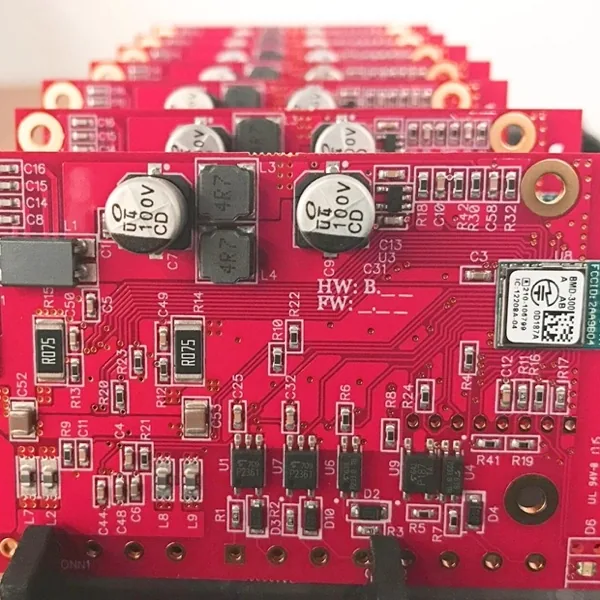
Short answer: Conformal coating is a thin film that follows the board contour and defends against moisture, dust and light chemical exposure while staying repairable. Potting fills the whole enclosure with a solid compound, adding mechanical, vibration and tamper protection — at the cost of weight, heat, and any hope of rework.
For reference, BELI Technologies offers conformal coating, potting and box-build as value-add steps on an assembly order; assembled boards up to 680 × 500 mm are inspected to IPC-A-610J, and there is no MOQ for prototypes.
Both processes exist on the same value-add menu at most electronics manufacturing services suppliers, including ours, and they get chosen for the wrong reasons more often than almost any other decision in a PCBA build. Teams specify conformal coating because a customer questionnaire asked about "environmental protection", or specify potting because a competitor's board looked impressively solid when they cut one open. Neither is a reason. This article works through what each process actually protects against, what it costs you in mass, heat and repairability, and how to decide — with the design and documentation detail your assembler will ask for once you do.
What does conformal coating actually protect against?
Conformal coating is a thin polymer film — typically tens of microns thick — applied over a populated board so that it conforms to the topography of components, leads and solder joints. Its job is to raise the surface insulation resistance of the assembly and keep contaminants away from the conductors underneath.
What it genuinely defends against: condensing humidity and the leakage currents that follow, airborne dust and fibres that bridge fine-pitch pads, salt fog in coastal and marine settings, light chemical and solvent splash, and the classic slow killer — electrochemical migration between adjacent conductors under bias in a damp environment. On a board with 0.35 mm lead pitch or a 0.4 mm ball-pitch BGA, the distance between two nets carrying a potential difference is small enough that a film of condensed moisture with a little ionic residue in it is a resistor you did not design.
What it does not do, and what buyers routinely assume it does: conformal coating is not an ingress-protection rating. IP67 or IP68 is a property of an enclosure and its seals, not of a 50-micron film on a PCB. Coating will not survive prolonged immersion, will not stop a connector filling with water, and will not hold pressure. It also does not protect anything it cannot reach — the underside of a BGA, the inside of a connector housing, the mating faces of a press-fit terminal. If your risk is submersion or high-pressure washdown, the answer is enclosure design, not a coating line item.
What is potting, and how is it different from encapsulation?
Potting means placing the assembly in a housing, shell or mould and filling the void with a curable compound — epoxy, polyurethane or silicone — until the electronics are entombed in a solid mass. The housing usually stays as part of the finished product. Encapsulation is the closely related process where the compound itself forms the outer body and the mould is removed, and glob-top is the same idea applied to a single die or a small cluster of parts rather than a whole board.
The distinction that matters commercially is that potting is a bulk process and coating is a surface process. Coating adds grams; potting adds tens to hundreds of grams and changes the product's centre of gravity, shipping class and sometimes its thermal design. Coating can be selectively applied and locally removed; potting is, for practical purposes, permanent. And potting delivers something coating cannot: mechanical support. A potted assembly resists shock and vibration because every component body is mechanically coupled to the housing rather than cantilevered off its solder joints. For a board that will spend its life on an engine mount, a compressor skid, or a handheld tool, that is often the real requirement, and moisture protection is a side benefit.
Potting is also the standard answer to two non-environmental problems: tamper resistance, because you cannot probe or desolder what you cannot see, and high-voltage insulation, because a filled gap has a far higher dielectric strength than the same gap full of air. Neither of those is a reason to coat.
Conformal coating vs potting: the decision table
| Dimension | Conformal coating | Potting / encapsulation |
|---|---|---|
| Level of protection | Humidity, condensation, dust, salt fog, light chemical splash. Not immersion, not pressure, not impact. | Everything coating covers, plus immersion within the compound's limits, shock, vibration, high-voltage isolation and tamper resistance. |
| Added weight & volume | Negligible — a film of tens of microns. No change to enclosure design. | Substantial. The compound fills every void; weight is driven by fill volume and compound density, and the housing must be designed around the pour. |
| Thermal behaviour | Slightly reduces convection from hot part surfaces; usually a second-order effect, but it matters on parts already running near their limit. | Eliminates internal air convection entirely. Thermally conductive compounds can improve conduction to the housing; unfilled ones can make hot spots worse. |
| Reworkability | Possible. Acrylics are the easiest to remove with solvent; urethanes and silicones are harder; parylene must be abraded or plasma-etched. All rework needs re-coating afterwards. | Effectively none. Assume any potted unit that fails is scrapped and budget the failure cost accordingly. |
| Cost direction | Dominated by masking labour and cure time, not by material. Cost per board falls sharply with volume once masking is systematised. | Dominated by material volume, mould or housing tooling, degassing and cure cycle. Cost per board is far less volume-sensitive. |
| Typical fit | Indoor-industrial, outdoor-sheltered, automotive cabin, IoT and metering devices, medical instruments, anything that may be repaired in the field. | Buried or submerged sensors, power supplies and drivers, high-vibration automotive and industrial modules, high-voltage assemblies, low-cost units with IP you want to hide. |
| Main failure mode to design against | Incomplete coverage — pinholes, thin edges, capillary bridging under low-standoff parts, and coating that crept where it was masked out. | Stress from CTE mismatch. A rigid compound shrinking on cure or cycling to low temperature can crack solder joints or lift components. |
Read the last row twice. Potting is the more aggressive protection, but it is also the process more capable of destroying an assembly that would otherwise have been fine. A hard epoxy poured around a tall electrolytic capacitor and then thermally cycled to minus 40 degrees will try to tear that capacitor off the board, and it frequently succeeds. That is why the compound's glass transition temperature, cure shrinkage and modulus matter more than its datasheet moisture-resistance figure.
Which coating material types exist, and where does each belong?
The material families below are general industry practice, not a menu of what any one factory stocks — settle the specific product and its qualification data with your supplier before you release a drawing. Cured film thickness is not a universal number either — it varies by material family and by the acceptance criteria you and your supplier agree in writing, so put the required range on the drawing instead of assuming a house default.
| Type | Strengths | Limitations | Typical environment |
|---|---|---|---|
| Acrylic (AR) | Easy to apply, fast drying, forgiving of process variation, and the simplest family to remove and re-coat during rework. Fluoresces well under UV for inspection. | Modest chemical and solvent resistance; limited abrasion resistance; not the choice for sustained high temperature. | Indoor and sheltered electronics, consumer and commercial gear, anything expected to be serviced. |
| Polyurethane (UR) | Strong moisture and chemical resistance, good abrasion resistance, durable film. | Much harder to rework than acrylic; some systems are moisture-cure and need controlled application conditions; can be brittle at low temperature. | Automotive, industrial control, fuel and solvent exposure, outdoor equipment. |
| Silicone (SR) | Widest service temperature range, stays flexible when cold, tolerates thermal cycling and vibration, good on assemblies with tall or heat-producing parts. | Soft and easy to damage mechanically; low-molecular-weight species can migrate and contaminate contacts, optics and sensors; usually applied thicker than other families. | High-temperature or wide-swing environments, LED lighting, power electronics, engine-adjacent assemblies. |
| Parylene (XY) | Vapour-deposited, so it reaches under low-standoff parts and into crevices that liquid coatings never wet. Very uniform, very thin, excellent dielectric and biocompatibility record. | Batch vacuum process, so cost per board is high and lead time is longer; every keep-out area must be physically masked; removal means abrasion or plasma, not solvent. | Implantable and diagnostic medical devices, aerospace, high-reliability sensors, dense assemblies where liquid coating cannot get underneath. |
| Epoxy (ER) | Hard, abrasion-resistant and chemically tough; the same chemistry family dominates potting compounds. | Rigid and essentially unremovable; shrinkage on cure puts stress on tall components; a two-part process with pot-life constraints. | Harsh mechanical and chemical environments where field repair was never on the table. |
Potting compounds map onto three of the same families. Epoxies give the hardest, most chemically resistant and most tamper-proof result and the highest internal stress. Polyurethanes sit in the middle: tougher than silicone, less brittle than epoxy, and generally the compromise choice for outdoor modules. Silicones are the softest and the kindest to solder joints under thermal cycling, which is why they dominate anything that must survive wide temperature swings, though they are also the easiest for a determined person to dig out.
When do you need neither?
This section exists because the most common mistake is specifying protection reflexively. If your product lives in a sealed enclosure in a climate-controlled room, coating buys you very little and costs you rework flexibility on every future field failure. Consider skipping both when all of the following hold: the operating environment is indoor and non-condensing; the enclosure already provides adequate dust protection; there is no salt, solvent or chemical exposure; the board is not subject to sustained vibration; and the assembly may realistically be repaired rather than replaced.
There is a cheaper intervention that resolves a surprising share of the moisture concerns coating is asked to solve: cleanliness. Ionic residue left on a board — from flux, from handling, from a poorly controlled process — is what turns condensation into leakage current. A properly cleaned, well-inspected assembly in a benign environment does not need a film. Conversely, coating over ionic contamination traps it against the copper and can make corrosion worse, not better, because the residue now sits in a humid microclimate it cannot escape. If you are considering coating primarily because you are worried about residues, fix the cleaning process first and then decide whether the film is still necessary.
The other honest answer is "not yet". Coating a prototype run rarely earns its keep, because you will be probing, cutting and reworking those boards. It is normal — and cheaper — to build engineering samples bare and introduce coating at the design-validation stage, once the layout is stable. Our walkthrough of EVT, DVT and PVT hardware build stages covers where each process change should land in that sequence.
Why is masking the biggest line item in a coating quote?
People assume conformal coating is priced on material. It is not. The film on a mid-size board costs very little; what you are paying for is the labour of deciding what must stay uncoated and then physically keeping the coating off it.
Every connector contact, test point, programming header, relay contact, potentiometer, switch actuator, LED lens, antenna, optical sensor window, MEMS microphone port, pressure sensor port, mounting hole with a grounding function and heatsink interface is a keep-out area. Each one has to be masked with tape, boots, dots or dispensed peelable latex before coating, then de-masked afterwards, then inspected to confirm the coating did not creep under the mask and that the masked area is genuinely clean. On a densely connectorised board that is minutes of skilled manual work per unit, twice, and it does not get much faster at volume unless the design cooperates.
Which means masking cost is a design decision, not a factory decision. Things that make it cheap: grouping all keep-out features into a defined region of the board rather than scattering them; choosing connectors that accept an off-the-shelf boot; leaving clearance around every keep-out so a mask has somewhere to seal; and specifying selective coating with a clear boundary on the drawing rather than "coat everything except the connectors". Things that make it expensive: a test point in the middle of a coated area, a keep-out feature within a millimetre of a component that must be coated, and a drawing that leaves the boundary to the operator's judgement. Ask your assembler for feedback on this before you release the design. A DFM review comes with every order we take, and the coating keep-out drawing is worth putting in front of the PCB assembly team at the same time, while moving a test point still costs nothing.
How much repairability are you giving up?
Reworkability is the trade nobody quantifies until the first field return arrives. Frame it as a straightforward expected-cost question: what fraction of units will need intervention after coating or potting, and what does each intervention cost under each option?
With coating, rework is possible but never free. The coating over the target area must be removed by solvent, abrasion or thermal parting; the repair is performed; then the area is cleaned and re-coated, and the re-coated area rarely matches the original film in appearance or in thickness uniformity. That whole loop needs a documented procedure if the product is in a regulated category — an undocumented touch-up on a medical or automotive assembly is a traceability problem, not just a cosmetic one.
With potting, there is no rework loop. Cutting a potted module open destroys it and usually damages the board underneath. The correct planning assumption is that a potted unit which fails in service is a scrapped unit, which pushes the cost of quality entirely upstream. That is not an argument against potting; it is an argument for stronger electrical and functional test coverage before the pour. In-circuit test coverage, functional test against the product specification, and a burn-in run all become more valuable the moment repair stops being possible, because the only remaining defence is not shipping a bad unit in the first place. Our functional testing and ICT service targets at least 95 percent node coverage with fixtures built in two to three working days, and that coverage figure is worth negotiating harder when the product is going to be potted.
What does coating or potting do to thermal design?
Coating has a modest thermal effect: a thin polymer film slightly impedes convective and radiative heat transfer from a hot component surface. On most designs this is negligible. On a design where a regulator or power stage is already running within ten degrees of its limit, it is not, and the correct response is to measure rather than assume — coat a sample, instrument the hot parts, and compare.
Potting is a genuine thermal redesign. Filling the enclosure removes internal air movement entirely, so every watt now leaves by conduction through the compound to the housing wall. Whether that is better or worse than the air it replaced depends on the compound: thermally conductive filled compounds can substantially improve heat transfer out of a sealed box, while an unfilled compound with poor conductivity can trap heat around a part that used to shed it into circulating air. The same fillers that improve conductivity usually raise viscosity, which makes complete void-free filling harder around tall or closely spaced components. Sort this out at the design stage with thermal measurements on a potted sample, not by reading the compound datasheet.
Component height is also a physical constraint worth checking early. Our SMT lines handle component heights up to 25 mm and boards up to 680 by 500 mm, which sets the practical envelope for what can be assembled before any fill operation; the full envelope is on our manufacturing capability page.
How do you prove the protection actually works?
A coating or potting specification without an acceptance test is a hope, not a requirement. Two kinds of evidence matter.
The first is process evidence: coverage and thickness. Industry acceptance documents publish criteria for what counts as acceptable coverage, thickness and freedom from defects such as bubbles, delamination and dewetting, and many coatings include a UV tracer specifically so coverage can be verified under black light. Agree with your assembler which criteria apply to your product, what gets inspected on every unit versus on a sample, and what evidence you receive — the answer should be in writing on the quotation, not assumed.
The second is performance evidence: does a coated or potted unit still work after the environment does its worst? This is where environmental stress screening pays for itself. Temperature and humidity cycling is the direct test of a moisture barrier, thermal cycling exposes the CTE-mismatch cracking that potting compounds cause, and a burn-in run under bias surfaces the leakage failures that a marginal film allows. At BELI we run temperature testing from minus 40 to plus 85 degrees Celsius at 20 to 98 percent relative humidity and burn-in for up to 24 hours in-house, and test reports go out with every shipment — which means a coated or potted sample set can be screened on our own equipment instead of being shipped out to a third party and back before you have an answer. Where a formal qualification standard applies to your market, the accredited-lab work still belongs at a lab; the split of responsibilities is the same one described in our guide to CE, FCC and UL compliance for China-built PCBA.
What does your assembler need in order to quote it?
Coating and potting are the two value-add processes most likely to be quoted vaguely and then argued about later. A quotable package includes: the material family or a specific approved product; the required thickness range or fill depth; a marked-up drawing or a dedicated fabrication layer showing every keep-out area; the application method you expect, if you have a preference; the acceptance criteria and inspection method; whether the housing is supplied by you or sourced by the factory; and the cure and handling constraints that follow, since some systems need days of full cure before the unit can be boxed.
Two of those items drive most of the price. The keep-out drawing drives masking labour, as above. The fill volume drives potting material cost, and it is worth calculating rather than estimating, because compound is bought by mass and a housing with more void than you think will quietly double that line. If the housing and any thermal interface parts are to come through the factory rather than from you, treat that as a sourcing question as much as a process one, and put every one of those items on the BOM with a specific part number. On the electronic side, component sourcing through authorized distributors and original manufacturers keeps traceability intact; mechanical and enclosure items deserve the same level of specification so nothing is left to the buyer's interpretation. The rest of the quoting package is the same set of files described in what files are required for a PCBA quotation, and the cost structure it feeds into is broken down in our guide to PCBA cost in China.
A short decision path
If you want a single sequence to run through: start by writing down the actual environment — temperature range, condensing or not, chemical exposure, vibration profile, expected service life. Then ask whether the enclosure can solve it, because sealing is usually cheaper than filling. If the enclosure cannot, ask whether the threat is chemical and electrical only, or also mechanical. Chemical and electrical alone points to conformal coating. Add sustained shock, vibration, high voltage or a tamper concern and it points to potting. Finally, ask what happens when a unit fails in year two: if the answer is "we replace it", potting is on the table; if the answer is "we repair it", coat it and keep the repair path open.
The one thing not to do is specify either process late. Both change the drawing package, both change the enclosure, and potting can change the thermal design outright. Decide during design validation, prove it on a sample set, and freeze it before the production validation build.
If you are weighing conformal coating against potting for a board we could build for you, send us your design files and a description of the operating environment. We quote within 24 hours, include a DFM review with every order, and can tell you where the masking cost is hiding in your layout before you commit to it. Conformal coating, potting and box-build are all available as value-add steps on the same lines that run SMT and through-hole assembly, with no MOQ for prototypes. If the board is going into a control cabinet or onto a machine, our industrial automation PCBA page covers how coating fits alongside the other countermeasures industrial hardware leans on.
Related reading: EVT, DVT, PVT: Hardware Build Stages and Your EMS · Key Questions to Ask Before Outsourcing PCBA · How Much Does PCBA Cost in China