
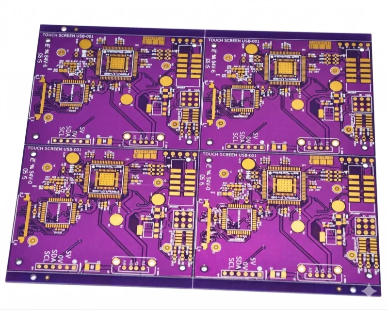
Short answer: A complete Gerber package contains every copper, solder mask, silkscreen and paste layer, a separate drill file, an unambiguous board outline, and a fab note stating stackup and finish — all in RS-274X with embedded apertures. Verify it by opening the exact zip you intend to send in an independent viewer.
Every PCB manufacturer has the same private statistic: the share of incoming jobs that cannot be quoted without an email asking for something. The missing item is rarely exotic. It is a drill file, a board outline, a layer whose function nobody can identify, or a set of coordinates that place the parts a few millimetres off the board. None of these are hard problems. They are simply invisible from inside the EDA tool, because the tool renders your design from its own database — not from the files you exported. This guide is deliberately not a menu-by-menu tutorial for KiCad, Altium or Eagle, because those menus move between releases and the screenshots rot within a year. Instead it describes what the output has to contain and how to prove it does, which is knowledge that survives every version bump.
What does a factory actually do with your Gerber files?
Understanding the downstream use explains most of the rules. A fabricator's CAM department imports your package, identifies each layer by its function, aligns everything to a common origin, and rebuilds a manufacturing dataset: photoplot data for imaging, drill programs for the mechanical and laser drills, routing paths for the profile, and a stencil aperture set if paste is included. Before any of that, they compare your geometry against process limits — trace and space, annular ring, drill-to-copper clearance, aspect ratio, mask sliver widths.
The critical point is that CAM works from your files, not your intent. If a layer is ambiguous, an engineer makes an interpretation and moves on, or stops and emails you. The first outcome costs you a wrong board; the second costs you two days. Both are avoidable at export time. At BELI Technologies, every PCB fabrication order includes a DFM review before production starts, and quotes are returned within 24 hours, 7 days a week — but a DFM review can only comment on what is present in the package. It cannot infer a drill file that was never exported.
RS-274X versus the old format: why apertures must travel inside the file
Gerber began as a plotter control language. In the original RS-274D form, the file contained only coordinates and D-codes — instructions to select "tool 12" and flash it at a location. What tool 12 physically was lived in a separate aperture list, often a plain text table, sometimes never sent at all. When that list went missing, a fabricator had no way to know whether a pad was a 60 mil round or a 2 mm square, and a job effectively arrived as a drawing with no scale.
RS-274X, sometimes called extended Gerber, solved this by embedding aperture definitions inside each file, along with the coordinate format and unit declarations. This is the format any modern EDA tool produces by default and the only one you should send. Gerber X2 goes further, adding standardised attributes that declare what each file is — top copper, inner layer 3, solder mask bottom — plus drill span and net names, so the layer-identification guesswork disappears entirely. If your tool offers X2 output, enable it: it removes an entire category of misinterpretation at zero cost to you.
A practical test settles the question. Open a copper file in a text editor. If you see percent-delimited aperture definition commands near the top declaring shapes and sizes, you have RS-274X. If you see nothing but coordinates and bare D-codes, you are shipping the old format and the aperture list is somewhere else — or nowhere.
What files must a complete Gerber package contain?
Extensions vary by tool, and that variation is normal. What matters is that every function below is present and identifiable. The extensions in the middle column are the conventions you will most often see, not a requirement.
| Layer or file | What it tells the factory | Common extension | If it is missing or wrong |
|---|---|---|---|
| Top copper | Component-side traces, pads and copper pours | .gtl, F_Cu.gbr, .art | Job stops immediately; nothing can be imaged |
| Bottom copper | Solder-side traces and pads | .gbl, B_Cu.gbr | Same; also the layer most often forgotten on single-sided-looking designs |
| Inner signal and plane layers | Every internal copper layer, in stack order | .g1 .g2, .gp1, In1_Cu.gbr | Wrong layer order produces a board that is electrically valid on paper and useless in practice |
| Solder mask, top and bottom | Where mask is removed to expose pads | .gts / .gbs | Fully masked pads, or a fabricator generating openings from your copper with guessed expansion |
| Silkscreen or legend, top and bottom | Reference designators, polarity marks, logos | .gto / .gbo | Blank board; assembly and field debug lose their only visual map |
| Solder paste, top and bottom | Stencil apertures for SMT assembly | .gtp / .gbp | Not needed for bare boards, required for a stencil; without it the assembler derives apertures from mask or copper |
| Board outline or profile | The exact routed edge, plus internal cutouts and slots | .gko, .gm1, .gml, Edge_Cuts.gbr | A frequent cause of a quoting hold; nobody can price a board of unknown size |
| Plated drill file | Every plated hole and via, with tool diameters | .drl, .txt, .xln (Excellon) | An unconnected board; pads exist but nothing is drilled or plated through |
| Non-plated drill file | Mounting holes and tooling holes that must not be plated | separate .drl or -NPTH.drl | Plated mounting holes, which can short a chassis screw to a plane |
| Drill tool table or drill map | Tool number to diameter mapping and hole counts | .drr, .rep, embedded header | Diameters have to be inferred; this is exactly how hole-size errors survive review |
| IPC-D-356 netlist | Your intended electrical connectivity | .ipc, .d356 | Optional, but it lets the fabricator prove their CAM interpretation matches your schematic before imaging |
| Fab drawing or README | Stackup, material, thickness, copper weight, finish, mask colour, impedance | .pdf, .txt | Defaults get applied — and defaults are how a controlled-impedance design becomes an uncontrolled one |
Why is the drill file the piece that most often goes wrong?
Drill data is separate from Gerber by history: it uses Excellon format, a different language with its own conventions, and it is exported through a different dialog in most tools. That separation is why it gets forgotten, and why its settings get missed even when it is present.
Three details deserve checking every time. First, plated and non-plated holes should be in distinct files or explicitly tagged, because plating a mounting hole changes its finished diameter and can create an unintended connection. Second, the tool table must be present, whether embedded in the file header or supplied as a drill report — this is the only place your hole diameters are stated in a machine-readable way. Third, confirm whether the diameters you exported are finished hole sizes or drilled sizes; plating reduces a hole by a measurable amount, and a tight-tolerance fit is where that difference stops being academic.
Process limits matter here too. BELI's fabrication runs to a minimum hole diameter of 4 mil with a maximum aspect ratio of 11:1, so on a thick board the smallest drillable via is set by thickness as much as by the drill itself. If your design pushes those numbers, say so in the fab note rather than letting CAM discover it — the full set of limits is published on the manufacturing capability page.
Where is the board outline, and how does the factory know?
Gerber has no concept of "this is the edge of the board". The outline is just geometry on a layer, and the fabricator identifies it by convention or by an attribute. Three rules make it unambiguous.
Draw the profile as a single closed contour with no gaps and no double-drawn segments. A 0.01 mm gap invisible on screen is a break in the contour, and a CAM engineer either has to close it manually or ask you which side is inside. Put nothing else on that layer — no dimension arrows, no title block, no courtyard outlines — because everything on the outline layer is a candidate for being routed. And state the line width convention: most fabricators treat the outline as the centreline of the routing path, so a thick outline drawn as a decorative border invites a board that is off-size by half a router bit.
Internal features follow the same logic. Cutouts and slots must be closed contours on the outline layer, or defined as slots in the drill file, and it is worth saying in the fab note which method you used. Rounded corners, castellations and edge plating all need to be called out in words as well as drawn, because they change process steps rather than just geometry.
Panelization: state your intent before the factory chooses for you
Small boards are not built one at a time. They run in arrays, and the array design affects both fabrication yield and assembly feasibility. You have three options and should pick one explicitly: supply a fully panelized dataset, supply a single board and specify the panel parameters you want, or supply a single board and ask the factory to propose the most economical panel.
If you choose the first, the package needs to show the panel outline, the individual board outlines, rails, tooling holes and global fiducials. If you choose the second, specify the separation method — V-score for straight-edged boards, tab-route with perforations for boards with irregular profiles or overhanging connectors — plus the array count and rail width. If you choose the third, say so in writing; a request to "panelize as you see fit" is a valid instruction, an absence of any instruction is not.
One constraint links panelization to assembly directly. BELI's SMT lines handle boards from 45 x 45 mm up to 680 x 500 mm, so a board below that minimum needs to reach assembly in an array rather than as a single piece. Fiducials matter for the same reason: SMT machines use them for optical alignment, and a panel needs global fiducials on the rails in addition to local fiducials near fine-pitch parts. With placement precision of ±0.03 mm and BGA ball pitch down to 0.4 mm on our PCB assembly lines, alignment accuracy is limited by the reference marks in your artwork, not by the machine.
Units, coordinate format and precision: the silent corruption
Gerber and Excellon both encode coordinates as integers, with a declared format telling the reader where the decimal point sits. A 2.4 format in inches means two integer digits and four decimals. Older files sometimes use leading or trailing zero suppression, dropping zeros to save bytes on 1970s media. Get that declaration wrong on import and every coordinate scales by a factor of ten — a mistake that produces a plausible-looking plot rather than an obvious error, which is precisely what makes it dangerous.
Modern practice removes the risk. Export in metric with a 4.6 format, use absolute coordinates, and disable zero suppression. Keep the same units across the Gerber set, the drill file and the pick-and-place file: a package where the copper is metric and the drill file is imperial is legal, importable, and an invitation to a units error. Precision also has a floor worth knowing — exporting at 2.3 inch resolution quantises everything to a thousandth of an inch, which is coarse relative to the 3.0/3.0 mil inner-layer line width and spacing BELI can fabricate.
Why do pick-and-place coordinates end up offset or rotated?
This is the classic assembly-side trap, and it has two independent causes.
The first is origin mismatch. Your centroid file states X and Y relative to some origin, and your EDA tool may use the drawing sheet origin, a user-defined origin, or the board origin depending on how the project was set up. If the Gerbers reference one origin and the centroid file another, every part is offset by a constant. The fix is to set the origin to a defined physical feature — the lower-left corner of the board outline is the safest convention — export everything from that same origin, and state it in the file header or the README. If the design is panelized, also state whether coordinates refer to the single board or the panel.
The second is rotation reference. Rotation in a centroid file is measured from the footprint's own zero-degree orientation as defined in your library, and library authors do not always follow the pin-1 conventions in IPC-7351. A tantalum capacitor footprint drawn with the anode to the right in one library and upward in another will export different rotation values for visually identical placements. The consequence lands on polarised parts — diodes, electrolytics, connectors, and any IC where pin 1 orientation is not obvious from the package outline.
Two habits eliminate almost all of it. Send an assembly drawing or a top-and-bottom 3D render showing pin-1 and polarity markers, so the machine program can be checked against a picture instead of a number. And state your bottom-side convention: some tools give bottom-side coordinates as viewed from the top through the board, others as viewed from below, and mirroring the wrong way puts every bottom part in the wrong place. The BOM, centroid file and Gerbers should all be exported from one design revision, with reference designators that match across all three — our guide to the files required for a PCBA quotation covers the BOM structure in detail.
What do ODB++ and IPC-2581 do better than Gerber?
Gerber describes each layer in isolation. Nothing in a plain Gerber set states how many layers there are, what order they sit in, which are planes, or what the board is supposed to connect. Every one of those facts is reconstructed at the factory from filenames, conventions and your notes — which is where interpretation errors are born.
ODB++ and IPC-2581 replace the loose collection with a single structured database. One file carries the layer stack in order with each layer's function declared, drill spans, the netlist, the profile, and optionally component data including placement and BOM references. IPC-2581 has the additional merit of being an open, vendor-neutral standard rather than a format controlled by one EDA vendor. In practice the benefit is measured in the questions that never get asked: no layer-order query, no plane-polarity query, no "is this file the outline or a mechanical drawing" query.
None of this makes Gerber obsolete. It remains the universal exchange format, every fabricator on earth reads it, and RS-274X with X2 attributes closes much of the gap. BELI quotes from either Gerber or ODB++. The practical recommendation is simple: if your tool exports ODB++ or IPC-2581 cleanly, send it alongside the Gerber set. The redundancy costs you nothing and gives the CAM engineer a cross-check.
How do you self-check a Gerber package in ten minutes?
The single most valuable habit in this entire article: open the exact zip file you are about to send in an independent viewer — a free standalone Gerber viewer, or a fabricator's online preview — and inspect it as if you had never seen the design. Your EDA tool renders its internal database, so it will show you a correct board even when the export is broken. A viewer shows only what the files contain, which is what the factory will see.
| Check before you send | How to verify it | Why it matters |
|---|---|---|
| Layer count matches your stackup | Count copper files in the zip; compare to the layer count in your fab note | A missing inner layer is invisible in a top-down view and fatal in production |
| Layer order is documented | Name files with explicit ordering, or state the order in the README, or use X2 attributes | Filename conventions differ between tools; nobody should have to guess which file is layer 3 |
| Drill file is present and aligned | Overlay drill on copper in the viewer; every hit should sit centred in a pad | Catches both a missing file and an origin mismatch between drill and Gerber |
| Hole diameters are what you think they are | Read the tool table; measure two or three holes against the mating part datasheet | Fractions of a millimetre decide whether a connector inserts or has to be forced |
| Board outline is one closed contour | Zoom to each corner in the viewer; look for gaps and stray objects on that layer | Open contours stop CAM; stray objects get routed into the board |
| Cutouts and slots are defined once | Confirm each is either a closed contour on the outline layer or a slot in the drill file, not both | Duplicated definitions produce oversized or double-routed features |
| Files are RS-274X | Open a copper file in a text editor and look for embedded aperture definitions | Old-format files without an aperture list cannot be manufactured as sent |
| Units and coordinate format are consistent | Check the format declaration in each file; metric 4.6, absolute, no zero suppression | Mixed units and zero suppression cause silent factor-of-ten scaling errors |
| Every SMD pad has a mask opening | View mask over copper; look for pads still covered, especially under connectors and shields | A masked pad is an open circuit that assembly cannot recover |
| Silkscreen is clipped off pads | View legend over mask; look for text crossing exposed copper | Ink on a pad degrades solderability; fabricators clip it, and clipping can erase a designator |
| Plane layers render with correct polarity | Confirm planes appear as solid copper with clearances, not as inverted artwork | Legacy negative-plane exports invert the entire layer if the polarity is misread |
| Panel intent and fiducials are stated | Confirm array method, rails, tooling holes and global fiducials, or an explicit request to panelize | Assembly alignment and separation method are both set here, not later |
| Centroid origin and rotation are declared | State the origin feature and the bottom-side viewing convention in the file header | Prevents whole-board offsets and rotated polarised parts |
| The zip contains only the current revision | Export to a clean empty folder every time; never zip a working directory | Stale files from a previous export are the most avoidable defect in this list |
That last row deserves its own emphasis. Exporting into a folder that already contains yesterday's output is how a superseded inner layer or an obsolete drill file ends up in a package that otherwise looks perfect. Delete and recreate the output folder as part of the export routine.
What does a small dimensional error actually cost?
The abstract case for checking your files is easy to nod at and easy to skip. The concrete one is more persuasive. A US smart-sensor customer came to us after boards had already shipped, with a problem that only appeared at final assembly: technicians could not insert components without excessive force, risking pad lift, lead deformation and cracked joints. The DFM review traced it to the Gerber package itself — the drill diameters had been specified at 0.8 mm, without allowance for the insertion tolerance the connectors required. We enlarged the holes to 1.2 mm, changed the connector to pin headers for a reliable tool-free mating, and turned the fix around in 48 hours with zero rework. The full account is in our Gerber hole issue case study.
Note where the error lived. Nothing was wrong with the fabrication; the board matched the files exactly. The gap was between what the files said and what the designer assumed they said — 0.4 mm of it. That gap is what an independent viewer check and a hole-diameter cross-reference against the mating part's datasheet are designed to catch, and it is why generic design standards such as IPC-2221 publish lead-to-hole clearance guidance rather than leaving it to judgement.
What to send with the Gerbers, and what a DFM review catches afterwards
Gerber describes geometry and nothing else. Everything about materials and process lives outside it, so a short fab note — a PDF drawing or even a plain text file — should accompany every package. Cover the layer count and stack order, base material and Tg, finished board thickness, copper weight on outer and inner layers, surface finish, solder mask and silkscreen colours, any controlled-impedance requirements with target values and tolerance, and the quantity and delivery expectation. BELI fabricates up to 42 layers, in materials including FR-4, High-Tg FR-4, halogen-free laminates, Rogers, Arlon, Taconic and Nelco, with surface finishes including ENIG, HASL, lead-free HASL, immersion silver and immersion tin, and holds impedance control to ±10% — but only if the requirement is written down, since none of it is inferable from copper artwork.
For an assembly quote, add the BOM with manufacturer part numbers, the centroid file, and any assembly drawing that clarifies orientation. If you are early in a hardware programme, it is worth building this package discipline during your first prototype rather than at the pilot build, because the same dataset carries forward through EVT, DVT and PVT stages and gets re-exported at every revision. If the distinction between a bare board order and an assembled one is still fuzzy, our explainer on PCB versus PCBA sets out what each stage requires.
No export checklist catches everything, which is why the file check and the manufacturing review are complementary rather than redundant. Your viewer check catches what is missing or misdeclared; a fabricator's DFM review catches what is present but unmanufacturable — annular rings too thin after drill tolerance, clearances below process limits, mask slivers that will not survive development, aspect ratios beyond what plating chemistry can fill.
BELI Technologies includes a DFM review with every fabrication order, quotes within 24 hours, and takes Gerber or ODB++ for quoting, with no MOQ on prototypes. Quick-turn bare boards run as fast as 24 hours for 1-2 layer designs and typically 3-7 working days for multilayer, and prototype assembly takes 48 hours once boards and parts are on site. If you are not certain your export is complete, send us the package you have — the review will tell you exactly what is missing before it costs you a build.
Related reading: What Files Are Required for PCBA Quotation · How We Fixed a Gerber Hole Issue for a Sensor Client · Prototype PCBA in China: A Practical Guide