
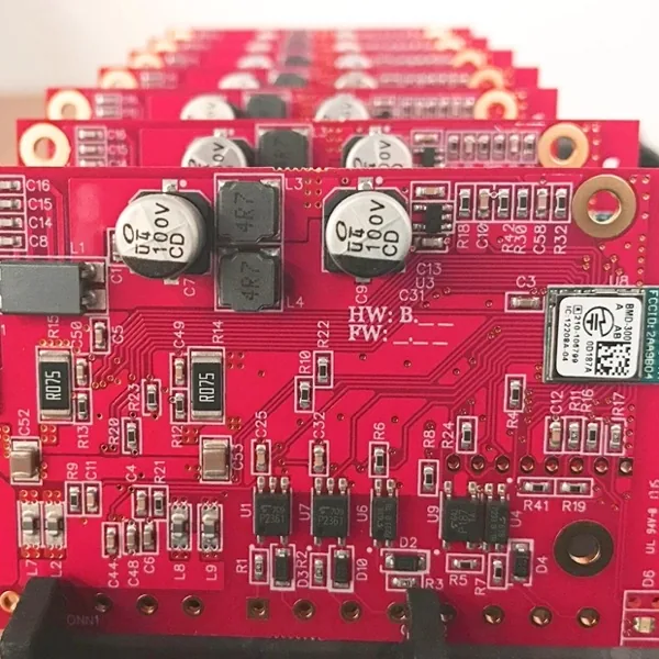
Short answer: surface-mount technology (SMT) solders components directly onto pads on the board's surface; through-hole technology (THT) inserts component leads through drilled, plated holes and solders them on the far side. SMT is smaller, faster to place and far cheaper per joint at volume, which is why it carries the overwhelming majority of components on a modern board. Through-hole survives where mechanical strength or raw power handling matters — connectors, transformers, large capacitors — and most real products ship with both on the same board.
The distinction matters at two moments. When you design, it decides footprints, drill data and which side of the board parts can live on. When you send files for assembly quotes, it decides which processes — reflow, wave, selective, hand soldering — your board actually needs, and therefore what you pay. This guide defines both technologies, shows where each one wins, walks through how mixed boards are actually built, and ends with the file details that prevent expensive surprises.
SMT vs through-hole at a glance
| SMT (surface-mount) | Through-hole (THT) | |
|---|---|---|
| Mounting | Soldered onto surface pads | Leads through drilled, plated holes |
| Soldering process | Solder paste + reflow oven | Wave, selective or hand soldering |
| Typical parts | Chip resistors/capacitors, QFP, QFN, BGA, CSP | Connectors, transformers, large electrolytics, power devices, relays |
| Smallest packages in production | 01005 chips and 0.4 mm BGA pitch on the partner lines behind BELI's assembly service; specialised lines go smaller | Limited by lead and hole geometry |
| Board sides | Both sides usable | Leads occupy both sides by definition |
| Mechanical strength | Pad-level; adequate for most parts | Strongest — the plated barrel anchors the joint through the board |
| Cost at volume | Lowest per joint (fully automated) | Higher per joint (insertion + second process) |
| Hand prototyping / rework | Harder below 0603; BGA needs X-ray | Easy with an iron; friendly to field repair |
What is SMT? Components on the surface
Surface-mount technology places components onto pads printed with solder paste, then melts the paste in a reflow oven so every joint forms at once. The production sequence is rigid and highly automated: solder paste is squeegeed through a laser-cut stencil onto the pads, solder paste inspection (SPI) verifies the deposit, pick-and-place machines set each component into the wet paste, and the populated board travels through a reflow oven whose temperature profile — preheat, soak, reflow, cooling — is tuned to the solder alloy and the board's thermal mass. Automated optical inspection (AOI) then checks every visible joint, and X-ray inspection verifies the hidden ones under BGAs and QFNs.
The parts themselves are surface-mount devices (SMDs): chip resistors and capacitors down to 01005, small-outline transistors and ICs (SOT, SOIC), quad flat packages with and without leads (QFP, QFN), and area-array packages (BGA, CSP) whose solder balls sit entirely under the body. Because nothing pokes through the board, both sides are available for placement, and the same square centimetre of board carries far more circuitry than through-hole layout ever could.
Speed is the other half of the story. Placement machines set parts in fractions of a second — the partner SMT lines behind BELI's assembly service run at 0.15 seconds per chip with ±0.03 mm accuracy, down to 01005 components and 0.4 mm-pitch BGAs — which is what makes a board with eight hundred components economically routine rather than a heroic soldering exercise.
What is through-hole? Leads through the board
Through-hole technology is the older method: component leads pass through drilled holes whose walls are plated with copper, and solder fills the gap between lead and barrel — on the far side and, ideally, up through the hole itself. The result is a joint anchored by a metal cylinder that runs the full thickness of the board, not just a pad sitting on its surface. That geometry is why through-hole parts shrug off forces that would peel a surface pad away.
Soldering happens in one of three ways. Wave soldering passes the board's underside over a standing wave of molten solder and does every through-hole joint in one pass — the volume process. Selective soldering uses a programmable miniature solder fountain to hit individual joints, the right tool when a mostly-SMT board carries a handful of through-hole parts and a full wave pass would disturb them. Hand soldering remains entirely respectable for prototypes, repairs and low volumes.
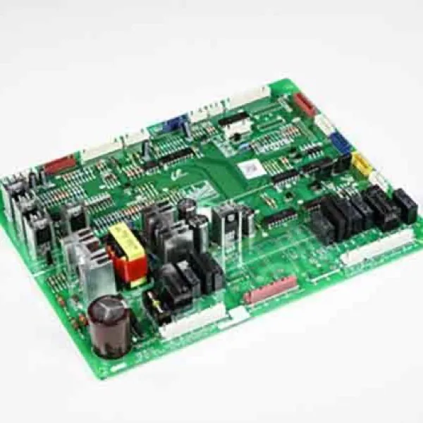
The parts that stay through-hole in 2026 do so for physics, not nostalgia: connectors that get plugged and unplugged for years (USB ports, headers, power jacks), transformers and large inductors whose mass would tear off a surface pad in vibration, bulk electrolytic capacitors, TO-220/TO-247 power packages bolted to heatsinks, relays, and fuse holders. If a part transfers force or serious current into the board, a plated barrel is still the strongest way to hold it.
Where each technology wins
| Your priority | Better fit | Why |
|---|---|---|
| Miniaturisation / density | SMT | Smaller packages, both board sides, no drilled real estate |
| High-frequency signal paths | SMT | Short or no leads mean lower parasitic inductance and capacitance |
| Unit cost in production | SMT | Fully automated placement; cost per joint falls with every thousand boards |
| Connectors and anything plugged/unplugged | THT | Insertion force goes into the plated barrel, not a surface pad |
| Vibration, drops, heavy components | THT | Mechanical anchoring through the full board thickness |
| High power / high voltage parts | THT | Big packages, heatsink mounting, creepage managed with lead spacing |
| Hand-built prototypes and field repair | THT | An iron and a steady hand suffice; no stencil, no reflow profile |
Notice what is missing from the table: reliability as a blanket category. A properly formed SMT joint is not a fragile joint, and modern electronics — phones surviving pockets and drops, automotive modules surviving engine bays — are overwhelmingly surface-mount. The honest engineering statement is narrower: for parts that concentrate mechanical load or heat, the through-hole barrel still wins. For everything else, SMT reliability stopped being the question decades ago.
Most real boards are both: mixed-technology assembly
Open almost any product — the router on your shelf, an industrial controller, a medical pump — and the board inside is mixed-technology: hundreds of SMT parts and a modest population of through-hole connectors and power components. That mix dictates the build order, because each soldering process must not destroy the joints made before it.
| Step | Process | What happens |
|---|---|---|
| 1 | SMT, side one | Paste print → place → reflow the side with the smaller, lighter components first |
| 2 | SMT, side two | Repeat on the reverse; heavy parts and large BGAs go here so they see one reflow upright, while surface tension holds the lighter side-one parts hanging through it |
| 3 | Through-hole insertion | Connectors, electrolytics and power parts inserted by hand or machine |
| 4 | Wave or selective solder | Full wave if the underside allows it; selective fountain if SMT parts occupy it |
| 5 | Inspection & test | AOI on solder joints, X-ray under BGAs, then ICT or functional test |
Two refinements are worth knowing. Pin-in-paste (intrusive reflow) prints paste into the through-holes themselves, inserts the leaded parts before the oven, and reflows everything in one pass — eliminating the wave step for boards with only a few compatible through-hole parts. And when the underside carries SMT chips that must survive a wave pass, they are glued down and the wave washes over them — a constraint your assembler will flag at the quoting stage if the layout forces it.
What the choice does to cost
SMT concentrates its cost up front. A production run needs a stencil, machine programming and feeder setup — one-time charges that appear on every PCBA quotation as NRE. Once running, the marginal cost of an SMT joint is close to negligible: placement is measured in fractions of a second and thousands of joints reflow simultaneously. High volume is where SMT's economics become untouchable.
Through-hole spends its money per board instead. Insertion is often manual, wave soldering is a second process with its own setup, and selective soldering trades speed for precision. On a prototype the difference barely registers — a handful of hand-soldered joints is cheap. At ten thousand units, every unnecessary through-hole part is a recurring tax. This is why design-for-manufacturing reviews so often ask one blunt question: does this part truly need to be through-hole, or is it only through-hole because the library footprint was?
What the choice does to your files
For the SMT side, the assembler needs the paste layer in your Gerber export (it becomes the stencil), a centroid file with rotation and side for every part, and a BOM whose manufacturer part numbers resolve to real, orderable packages — the requirements covered in what files a PCBA quote needs.
For the through-hole side, the critical dimension is the relationship between lead diameter and finished hole size. The plating that makes a barrel solderable also narrows it, and a hole specified without insertion clearance produces boards that match the drill file perfectly yet reject their own connectors on the assembly bench. We have seen exactly this failure: a 0.8 mm drill spec that blocked connector pins at final assembly — fixed by opening the holes to 1.2 mm and changing the connector to a standard pin header, with the standing rule since: verify every through-hole part's finished hole size against the mating part's datasheet. Annular ring width and hole-to-copper clearance follow the same rule: they are manufacturing dimensions, and the mating part's datasheet — not the footprint library — is the authority.
Sorting out the vocabulary
The terms tangle easily, so here is the untangling. SMT is the process; an SMD is the device the process places — a chip resistor is an SMD, reflow is SMT. THT names the through-hole process; you will also meet PTH (plated through-hole), which strictly describes the plated barrel itself — on plated boards every THT joint uses a PTH, but PTHs also exist purely as vias that route signals between layers and never receive a component lead. A leaded part in this context means one with wire leads for through-hole mounting — nothing to do with lead-free solder alloys, which both SMT and THT use routinely. And if a datasheet says a part is offered in radial or axial form, both are through-hole: radial leads exit one face side by side, axial leads exit opposite ends along the part's axis.
What this means when you request a quote
You rarely choose between SMT and through-hole for a whole board; your component selection has already chosen for you. What you can do is state the mix clearly. Tell the assembler roughly how many SMT placements and how many through-hole insertions the board carries, flag anything unusual — bottom-side through-hole parts, press-fit connectors, parts that must survive wave contact — and send the paste layer, centroid and BOM together so the quote reflects the processes your board actually needs. A turnkey assembly partner whose service spans SMT, wave and selective soldering will price the whole sequence in one pass, and a good DFM review will tell you if any through-hole part on the BOM could become surface-mount and save money at volume — or if a connector you specified as SMT is going to need the mechanical anchoring only a barrel provides.
Related reading: ENIG vs HASL: Which PCB Surface Finish Should You Choose? · PCB vs PCBA: What's the Difference? · What Files Are Required for PCBA Quotation · How We Fixed a Gerber Hole Issue for a Sensor Client