As for the PCBs, the double-sided PCBs are widely used in electronics manufacturing and are used for various devices starting with mobile phones and ending with large industrial equipment.
In modern electronics, their importance is relevant due to their ability to allow the incorporation of complex circuits within a small space. when it comes to double-sided PCBs, there is a serious emphasis on the considerable level of skill, as well as timing and adherence to the essential standards to guarantee their performance and effectiveness.
Here we are providing you with an extensive guide in which we share a step-by-step approach to double sided PCB assembly along with some tips and tricks to enhance the assembly line and get the best results out of it.
The Process of Double-Sided PCB Assembly
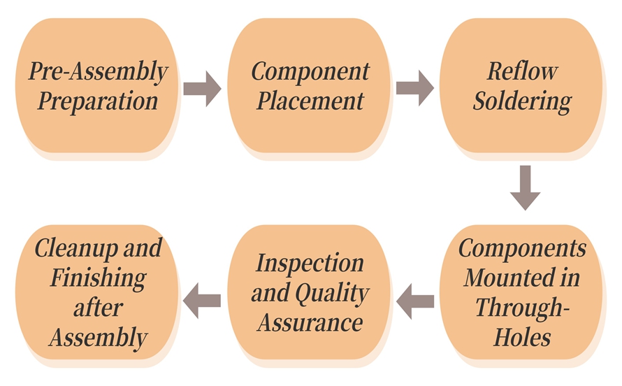
Step 1: Pre-Assembly Preparation
It is very crucial to have well-planned strategies and procedures that should be followed before we are going to engage in the process of double sided PCB assembly. This begins with collecting all the required parts, instruments, and papers.
Make sure that you have a BOM and component/assembly drawings to illustrate their locations and orientations.
After that, look through the surface to identify occasional bumps or any other signs of the solder mask misalignment, and copper traces that may be fixable at this stage. These issues should be corrected before double sided PCB assembly is attempted to prevent possible problems.
Arrange the required components neatly in one place in a methodical manner. Sufficient lighting, anti-static work surfaces and the use of microscopes or magnifying lamps respectively should not be missed in the double sided PCB assembly.
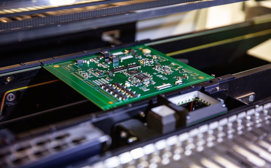
Step 2: Component Placement
The first part of double sided PCB assembly is putting the elements on one particular part of the board. Start with solder paste by applying it on the correct pads using stencils or dispensers. In the double sided PCB assembly, solder paste plays the role of the adhesive which is used to hold surface-mount components in place during a process known as reflow soldering.
With the help of precision placement equipment like the pick and place machines or by using manual tweezers fix the SMD components at the center of the solder paste applied on the pads.
Now, Focus on the particular position of the components with regard to the assembly drawings and polarity markings.
After all the SMD are soldered in the double sided SMT assembly, switch to THT on the same side of the PCB. Place leads of through-hole components into their respective through holes, ensuring that through-hole components are properly aligned to the component pads on the other side of the board.
Step 3: Reflow Soldering
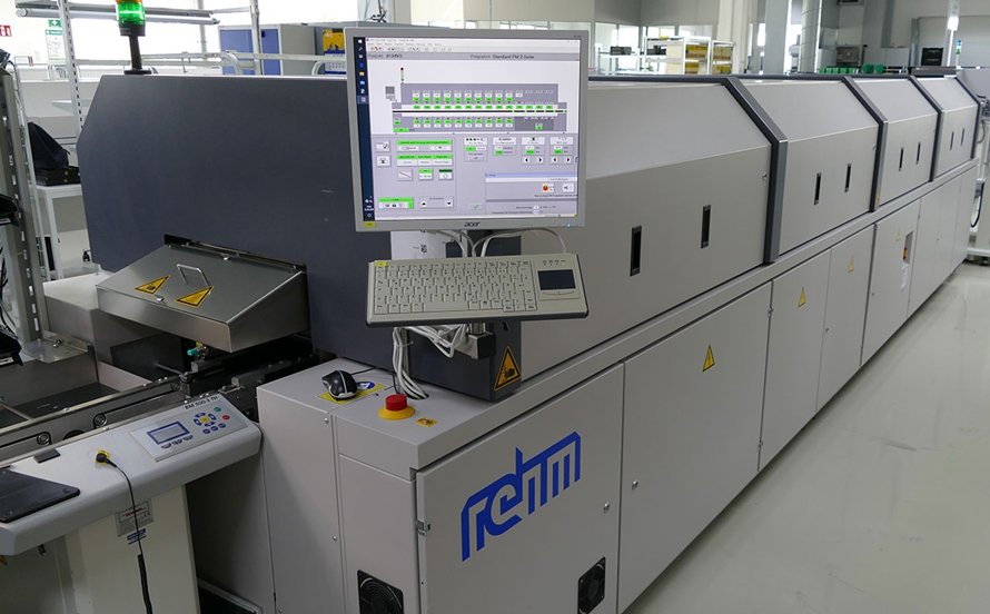
Double sided PCB soldering is achieved by double sided reflow soldering. During the double sided PCB reflow soldering process, the PCB is exposed to a preheating oven to a continuously increasing temperature until a sufficient temperature is attained. After that, the solder paste is reflowed, and the solder paste melts and reaches its maximum temperature. With slowly decreasing temperature, solder paste becomes rigid, creating permanent solder joints. This profile of double sided PCB soldering does a good job of making sure that solder flows and wet well, activating the flux, properly attaching the component to the board and does not apply extra heat stress on temperature-sensitive components.
Note:- In the double sided PCB assembly, supervise the double sided reflow soldering process keenly, especially the temperature profile of double sided reflow soldering to complement the solder paste specifications. Once double sided reflow soldering is done, do not immediately take the PCB out of the oven. otherwise, this will lead to thermal shock on the board damaging the solder joints.
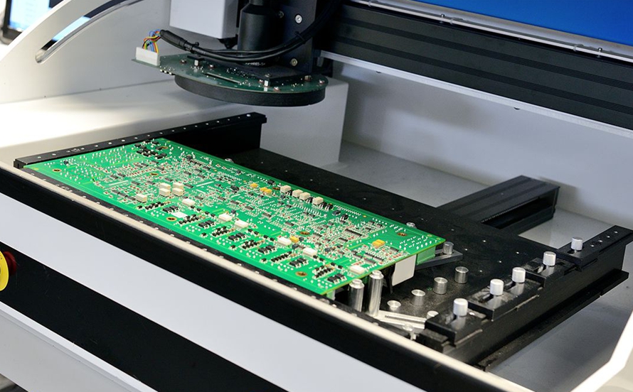
Step 4: Components Mounted in Through-Holes
After this kind of double sided PCB soldering, the focus shifts towards the through-hole components on the other side of the PCB, opposite to the double sided reflow soldering.
In the double sided PCB soldering of through-hole components, each of these components has to be soldered by hand to make electrical connections between the component leads and the PCB pads.
Start by cleaning through hole-barrel-filled solder joints for solder wetting. Next, with a soldering iron, matching the tip size and temperature, oxidize the solder joint while applying the solder to create a good electrical connection.
Note:- Pay attention during through-hole soldering in the double sided PCB assembly to avoid the overheating of some components, which yields their degradation and or sometimes damages the nearby circuits.
Step 5: Inspection and Quality Assurance
Inspection and quality assurance in the double sided PCB assembly are the most important practices used by assemblers for improvement in their current and future practice.
Once in the double sided PCB assembly, all the components have been soldered on the PCB, it is crucial to conduct an inspection or review of the assembly, this checks the quality of the assembly as well as identifies and inspects for any abnormalities.
Physical assessment in the double sided PCB assembly is done using simple optics like magnifying lenses, and microscopes. Using automatic optical inspection (AOI) on solder joints, proper positioning of the components and cleanliness of the printed circuit boards can be maintained.
Note:-Rework in the double sided PCB assembly should be done carefully with emphasis on areas like fine-pitch components, solder bridges and those regions of the board which contain a high density of components.
The performance of the equipment or material as well as its reliability can be impacted if there are any variations. Therefore, these areas should be noted down and receive appropriate action as soon as possible.
Another form of examination that is encouraged by most PCB assemblers, is functional testing which investigates the PCB’s working and electrical performance. In functional tests, continuity checks, and ICT tests may be performed to check whether assembled PCB is working according to design and complies with the functional, performance requirements.
Step 6: Cleanup and Finishing after Assembly
After completing the inspection and testing processes, it is necessary to clean and polish the assembled PCB so that it can be used for further processes. My final suggestion is to clean it from any flux cleaner or splatter which has proper solvents like IPA.
After cleaning the PCB, check for the presence of residual flux on the surface of the PCBs as it may cause corrosion, electrical leaking or occasional reliability problems in the future.
Last but not least, provide all those surface finishes in the double sided PCB assembly that may be required for improving the durability of the PCB, its ability to resist moisture and to protect the PCB from its environment. These techniques of finishing play a crucial role in protecting PCB against impurities like moisture, dust or any severe chemicals required for it to work in tough environments or different difficult conditions.
Conclusion
Over the past years, one of the most important manufacturing phases in almost all electronic equipment has been inserting components on both sides of the PCB and soldering them so that the required PCB can work according to its requirements. PCBs, until soldered with proper components, are like just a piece of metal plate which has few conducting paths. Assembling a PCB with all of its required components provides life to the PCB.
PCB manufacturing works best when it incorporates correct methods of assembly and the right quality checks as described in this article, therefore when implemented, it will help produce highly performing PCBs that will suit today’s versatile electronics market.
Comments are closed